- 您现在的位置:买卖IC网 > Sheet目录2003 > LTC1282ACN#PBF (Linear Technology)IC A/D CONV SAMPLING W/REF 24DIP
19
LTC1282
U
S
A
O
PPLICATI
WU
U
I FOR ATIO
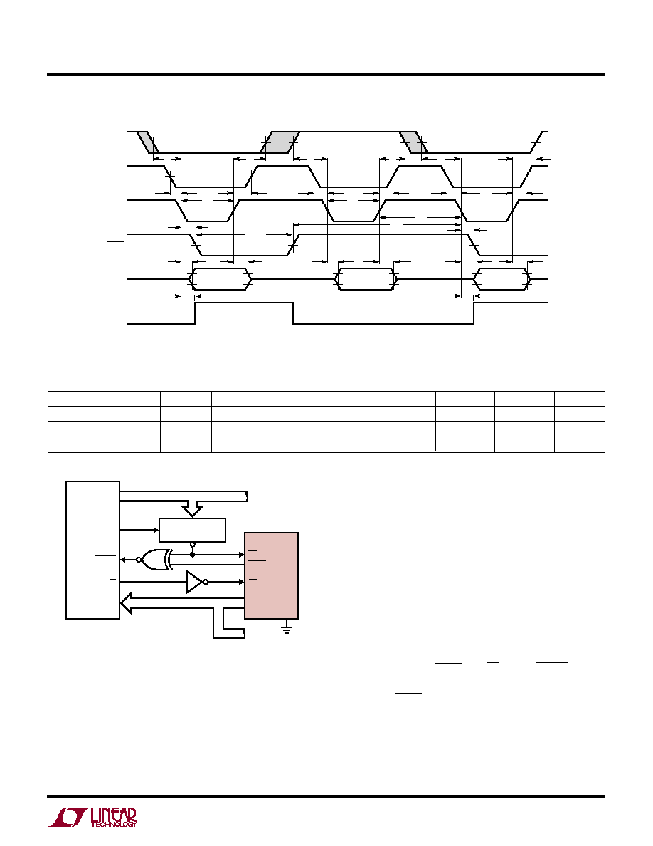
Figure 19. ROM Mode Two Byte Read Timing Diagram
Table 5. ROM Mode, Two Byte Read Data Bus Status
Data Outputs
D7
D6
D5
D4
D3/11
D2/10
D1/9
D0/8
First Read (Old Data)
DB7
DB6
DB5
DB4
DB3
DB2
DB1
DB0
Second Read (New Data)
Low
DB11
DB10
DB9
DB8
Third Read (New Data)
DB7
DB6
DB5
DB4
DB3
DB2
DB1
DB0
OLD DATA
DB7-DB0
NEW DATA
DB11-DB8
TRACK
HOLD
DATA
BUSY
RD
CS
RD
LTC1282 F19
t8
t1
t2
t3
tCONV
t11
t9
t8
t9
t5
t1
t4
t5
t10
t3
t7
t3
t7
t12
HBEN
t7
t4
t1
t8
t9
NEW DATA
DB7-DB0
t2
t4
t5
where D is Data Memory Address and PA is the PORT
ADDRESS.
MC68000 Microprocessor
Figure 21 shows a typical interface for the MC68000. The
LTC1282 is operating in the Slow Memory Mode. Assum-
ing the LTC1282 is located at address C000, then the
following single 16-bit MOVE instruction both starts a
conversion and reads the conversion result:
Move.W $C000,D0
At the beginning of the instruction cycle when the ADC
address is selected, BUSY and CS assert DTACK so that
the MC68000 is forced into a WAIT state. At the end of
conversion, BUSY returns high and the conversion result
is placed in the D0 register of the microprocessor.
Figure 20. TMS320C25 Interface
DATA BUS
LTC1282 F20
ADDRESS BUS
D0
D16
R/W
READY
IS
A1
A16
TMS320C25
ADDRESS
DECODE
EN
D0/8
D11
RD
BUSY
CS
HBEN
LTC1282
ADDITIONAL PINS OMITTED FOR CLARITY
发布紧急采购,3分钟左右您将得到回复。
相关PDF资料
LTC1288IS8#TRPBF
IC A/D CONV SAMPLING 12BIT 8SOIC
LTC1298IS8#TRPBF
IC A/D CONV SAMPLING 12BIT 8SOIC
LTC1327CNW#PBF
IC TXRX EIA/TIA-562 3.3V 28-DIP
LTC1329ACS8-50#TRPBF
IC D/A CONV 8BIT MICROPWR 8-SOIC
LTC1337CNW#PBF
IC 3DVR/5RCVR 5V RS232 28-DIP
LTC1382IN#PBF
IC TXRX 5V RS232 W/SHTDWN 18-DIP
LTC1383IS#TRPBF
IC TXRX 5V RS232 LOW PWR 16-SOIC
LTC1384IG#TRPBF
IC TXRX 5V RS232 LOW PWR 20-SSOP
相关代理商/技术参数
LTC1282ACSW
功能描述:IC A/D CONV SAMPLING W/REF24SOIC RoHS:否 类别:集成电路 (IC) >> 数据采集 - 模数转换器 系列:- 标准包装:1,000 系列:- 位数:12 采样率(每秒):300k 数据接口:并联 转换器数目:1 功率耗散(最大):75mW 电压电源:单电源 工作温度:0°C ~ 70°C 安装类型:表面贴装 封装/外壳:24-SOIC(0.295",7.50mm 宽) 供应商设备封装:24-SOIC 包装:带卷 (TR) 输入数目和类型:1 个单端,单极;1 个单端,双极
LTC1282ACSW#PBF
功能描述:IC A/D CONV SAMPLING W/REF24SOIC RoHS:是 类别:集成电路 (IC) >> 数据采集 - 模数转换器 系列:- 标准包装:1,000 系列:- 位数:12 采样率(每秒):300k 数据接口:并联 转换器数目:1 功率耗散(最大):75mW 电压电源:单电源 工作温度:0°C ~ 70°C 安装类型:表面贴装 封装/外壳:24-SOIC(0.295",7.50mm 宽) 供应商设备封装:24-SOIC 包装:带卷 (TR) 输入数目和类型:1 个单端,单极;1 个单端,双极
LTC1282ACSW#TR
功能描述:IC ADC 12BIT SAMPLING REF 24SOIC RoHS:否 类别:集成电路 (IC) >> 数据采集 - 模数转换器 系列:- 标准包装:1,000 系列:- 位数:12 采样率(每秒):300k 数据接口:并联 转换器数目:1 功率耗散(最大):75mW 电压电源:单电源 工作温度:0°C ~ 70°C 安装类型:表面贴装 封装/外壳:24-SOIC(0.295",7.50mm 宽) 供应商设备封装:24-SOIC 包装:带卷 (TR) 输入数目和类型:1 个单端,单极;1 个单端,双极
LTC1282ACSW#TRPBF
功能描述:IC A/D CONV SAMPLING W/REF24SOIC RoHS:是 类别:集成电路 (IC) >> 数据采集 - 模数转换器 系列:- 标准包装:1,000 系列:- 位数:12 采样率(每秒):300k 数据接口:并联 转换器数目:1 功率耗散(最大):75mW 电压电源:单电源 工作温度:0°C ~ 70°C 安装类型:表面贴装 封装/外壳:24-SOIC(0.295",7.50mm 宽) 供应商设备封装:24-SOIC 包装:带卷 (TR) 输入数目和类型:1 个单端,单极;1 个单端,双极
LTC1282BCN
功能描述:IC A/D CONV SAMPLING W/REF 24DIP RoHS:否 类别:集成电路 (IC) >> 数据采集 - 模数转换器 系列:- 其它有关文件:TSA1204 View All Specifications 标准包装:1 系列:- 位数:12 采样率(每秒):20M 数据接口:并联 转换器数目:2 功率耗散(最大):155mW 电压电源:模拟和数字 工作温度:-40°C ~ 85°C 安装类型:表面贴装 封装/外壳:48-TQFP 供应商设备封装:48-TQFP(7x7) 包装:Digi-Reel® 输入数目和类型:4 个单端,单极;2 个差分,单极 产品目录页面:1156 (CN2011-ZH PDF) 其它名称:497-5435-6
LTC1282BCN#PBF
功能描述:IC A/D CONV SAMPLING W/REF 24DIP RoHS:是 类别:集成电路 (IC) >> 数据采集 - 模数转换器 系列:- 产品培训模块:Lead (SnPb) Finish for COTS
Obsolescence Mitigation Program 标准包装:2,500 系列:- 位数:12 采样率(每秒):3M 数据接口:- 转换器数目:- 功率耗散(最大):- 电压电源:- 工作温度:- 安装类型:表面贴装 封装/外壳:SOT-23-6 供应商设备封装:SOT-23-6 包装:带卷 (TR) 输入数目和类型:-
LTC1282BCSW
功能描述:IC A/D CONV SAMPLING W/REF24SOIC RoHS:否 类别:集成电路 (IC) >> 数据采集 - 模数转换器 系列:- 标准包装:1,000 系列:- 位数:12 采样率(每秒):300k 数据接口:并联 转换器数目:1 功率耗散(最大):75mW 电压电源:单电源 工作温度:0°C ~ 70°C 安装类型:表面贴装 封装/外壳:24-SOIC(0.295",7.50mm 宽) 供应商设备封装:24-SOIC 包装:带卷 (TR) 输入数目和类型:1 个单端,单极;1 个单端,双极
LTC1282BCSW#PBF
功能描述:IC A/D CONV SAMPLING W/REF24SOIC RoHS:是 类别:集成电路 (IC) >> 数据采集 - 模数转换器 系列:- 标准包装:1,000 系列:- 位数:12 采样率(每秒):300k 数据接口:并联 转换器数目:1 功率耗散(最大):75mW 电压电源:单电源 工作温度:0°C ~ 70°C 安装类型:表面贴装 封装/外壳:24-SOIC(0.295",7.50mm 宽) 供应商设备封装:24-SOIC 包装:带卷 (TR) 输入数目和类型:1 个单端,单极;1 个单端,双极